


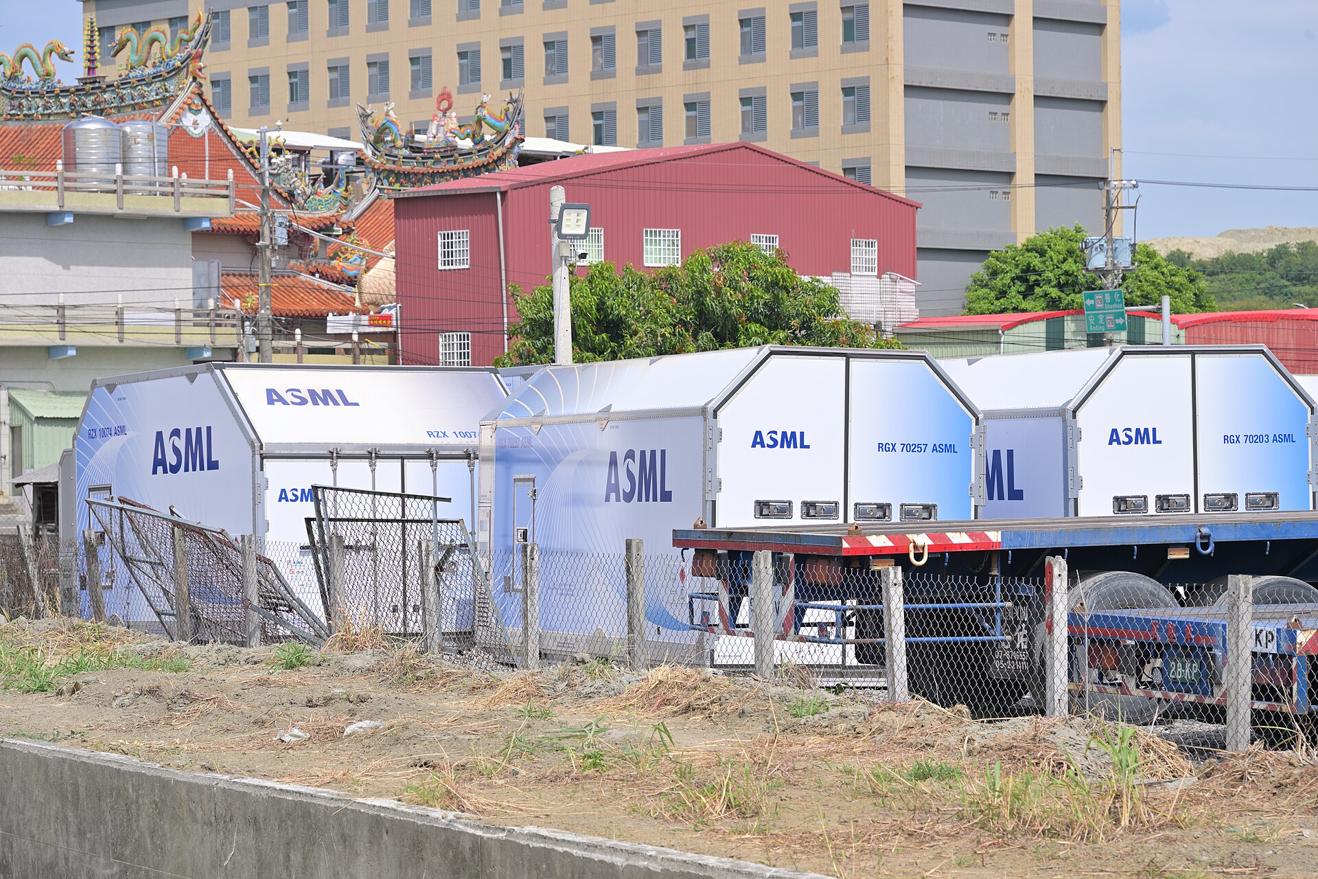
Elon Musk stated that ASML and other critical semiconductor equipment suppliers have expedited shipments for the Terafab semiconductor manufacturing facility. The announcement came during a live broadcast of SpaceX’s Q3 2026 earnings call on X on October 20. Musk emphasized that the project, a joint venture between Tesla and SpaceX, aims to achieve volume chip production at its primary site in Gibbons Creek, Texas, by the third or fourth quarter of 2028.
Musk described the timeline as highly aspirational with significant uncertainty. He noted that the aggressive schedule relies heavily on accelerated equipment deliveries from key partners. “These are very aggressive dates, and we’re very appreciative of ASML and all of our other suppliers in accelerating equipment deliveries in order to achieve this outcome,” Musk said.
ASML Equipment Delivery and Manufacturing Node
ASML holds the position of the world’s only commercial supplier of extreme ultraviolet (EUV) lithography systems, which are essential for high-volume leading-edge chip production. These systems carry a price tag of approximately $400 million each. Unofficial sources previously indicated that Terafab’s first EUV tool was slated for delivery in mid-2027. It remains unclear if the expedited timeline mentioned by Musk aligns with this earlier report.
The facility will utilize Intel’s 14A manufacturing node technology. Intel officially joined the Terafab venture in April 2026 to co-develop and refactor silicon fabrication technology. The project also involves other major equipment manufacturers, including Applied Materials, Lam Research, and KLA Corporation from the United States, as well as Tokyo Electron from Japan. These companies will provide front-end processing, metrology, and process control machinery.
Tesla and SpaceX are also negotiating with approximately ten South Korean equipment makers. These partners include Hanmi Semiconductor, known for advanced packaging equipment, and HPSP, which manufactures high-pressure hydrogen annealing equipment. Additional suppliers will provide specialized piping components and process valves.
Nvidia Vera Rubin Cluster and AI Compute Goals
Beyond the manufacturing facility, Musk outlined immediate ambitions for his artificial intelligence companies. He expects the combined AI infrastructure to reach 2.5 to 3 gigawatts of computing capacity by the end of 2026. Musk expressed high confidence in adding an incremental 10 gigawatts in 2027, stating he would be surprised if the total did not reach 13 gigawatts by the end of that year.
To support this expansion, SpaceX and xAI are procuring next-generation Nvidia architecture. Musk announced plans to bring a massive 440,000-GPU Nvidia “Vera Rubin” training cluster online by the end of the second quarter of 2027. This cluster will serve as the backbone for the company’s AI operations.
The Terafab facility aims to manufacture logic, memory, and advanced packaging internal architectures in a single location. The goal is to produce one terawatt of AI computing power annually. Musk claimed that the commercial value of the advanced chip output from this single building would place it within the top 20 global country gross domestic products. For context, the 20th country on that list is Switzerland, with a GDP of around $1.14 trillion.
SpaceX plans to manufacture its first experimental test chip at its research fabrication facility in Austin, Texas, around the second quarter of 2027. The chips produced at Terafab are intended to supply Musk’s xAI clusters, self-driving vehicles, Optimus humanoid robots, and SpaceX’s orbital AI data center.
Industry experts have questioned the validity of the one terawatt ambition. Research firm Gartner estimates the total global AI-optimized data center capacity at roughly 44 gigawatts as of late 2026. This figure represents only 4.4 percent of Terafab’s planned output. Global AI computing capacity has grown by roughly 3.3 to 3.4 times per year since 2022, according to EpochAI, but the scale of Terafab remains unprecedented.
Source: Tom’s Hardware
