


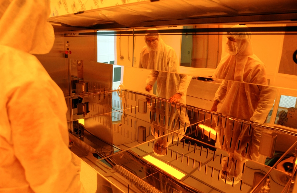
Russia-based Zelenograd Nanotechnology Center (ZNTC) has completed the third research and development stage of its first lithography tool capable of processing 200-mm wafers using 130nm process technology. The device is currently undergoing internal testing, but analysts and industry reports indicate it is still years away from being deployed in a real fabrication plant for mass chip production.
The project represents a significant engineering effort for the country’s microelectronics sector. According to documents reviewed by CNews, the Belarus-based company Planar was responsible for developing the lithography system, manufacturing mechanical assemblies, and commissioning the prototype. ZNTC handled the overall system development, design of test and process equipment, projection-lens calculations, and process modeling.
Development Costs and Component Sourcing
The Russian Ministry of Industry and Trade allocated approximately $70 million for the entire development program. The financial breakdown for a single unit suggests a 130nm-capable ZNTC stepper costs around $6.7 million, with the laser light source adding another $600,000. This brings the total cost of one tool to roughly $7.3 million.
To put these figures in perspective, ASML’s PAS 5500/150 stepper, which was launched in the first quarter of 2001, had a list price of $3.1 million. When adjusted for cumulative inflation of about 88%, that historical price translates to approximately $5.8 million in 2026 dollars. The Russian machine is a 200-mm system capable of 130nm fabrication technologies, a standard that Intel and AMD adopted in 2001 and 2002, respectively.
While blogger Dmitrii Kuznetsov has suggested the device is the first Russian 130nm-capable lithograph made entirely from domestic components, the supply chain appears more complex. Lasers for the unit were developed by Lassard, and Planar managed the mechanical and assembly aspects. It remains unclear whether the ZNTC stepper can be integrated into existing 130nm manufacturing nodes, as previous Russian efforts relied on ASML equipment. ZNTC claims to be developing the process technology around the machine, which likely involves qualifying the lithographic process, including resist selection, exposure dose, focus windows, masks, and alignment parameters.
Timeline for Commercial Deployment
Despite the completion of the prototype, the path to actual chip production is long. The first prototype was delivered five months later than originally scheduled. It is now undergoing internal engineering and acceptance testing. Following this phase, ZNTC must finalize the design and validate imaging, overlay, reliability, and throughput. This validation process is expected to take well over a year.
Even established lithography suppliers typically require several years to move from the first integrated engineering system to production deployment. A realistic timeframe for the Russian machine to begin processing commercial wafers is around 2029 at the earliest. Limited production of the steppers themselves could potentially begin earlier if ZNTC has all the required parts, but this would not constitute qualification for volume semiconductor manufacturing.
Alexander Mikhailov, an analyst with Strategy Partners, told CNews that the creation of a prototype for a domestically developed photolithography system is an important milestone. He noted that it demonstrates Russia has the engineering expertise required to develop such equipment and opens the door for systems targeting smaller process nodes, such as 90nm and 65nm.
For now, the ZNTC 130nm step-and-repeat system remains an engineering prototype. The next major step involves building prototype machines for actual chipmakers, who will then need to characterize them and qualify them for their specific production flows. This final stage could take months or even years to complete.
Source: Tom’s Hardware
